
Precision plays a crucial role in the semiconductor industry as it directly impacts device performance, functionality, and reliability. In this ever-evolving field, one technology that stands out in achieving precision is Chemical Mechanical Planarization (CMP). CMP wafers, in particular, play a significant role in enhancing device performance. In this article, we will delve deeper into the importance of precision in semiconductor devices and explore how these devices contribute to achieving that precision while enhancing device performance.
Importance of Precision in Semiconductor Devices

In the rapidly advancing semiconductor industry, precision is of utmost importance due to the increasing complexity of semiconductor devices. As transistors and components continue to shrink in size, precision becomes essential during the manufacturing process. Even minor variations or defects can have a significant impact on device yield, performance, and reliability. Therefore, achieving precision in device fabrication is a constant pursuit.
Understanding CMP Wafers
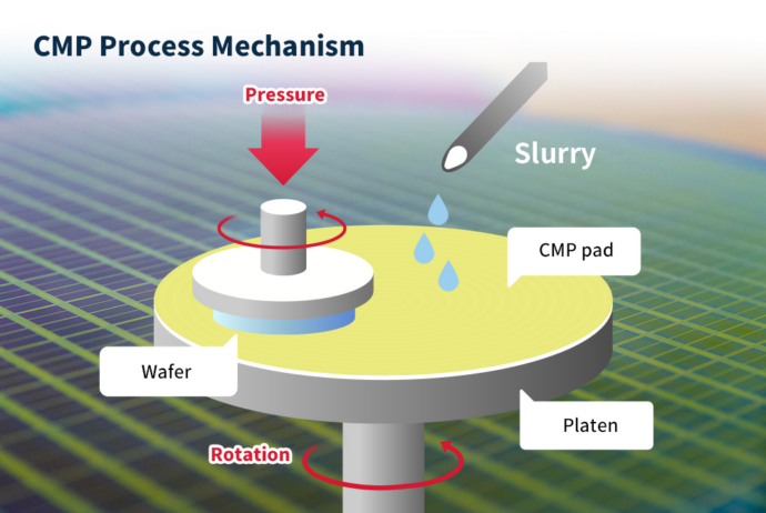
CMP wafers are integral to the semiconductor manufacturing process, specifically in Chemical Mechanical Planarization. These wafers, typically made of silicon or other semiconductor materials, possess a flat and highly polished surface. CMP wafers serve as a reference surface during the planarization process, allowing for the removal of excess material and the attainment of a uniform surface.
Enhancing Semiconductor Device Performance
CMP wafers bring several notable benefits that enhance semiconductor device performance in various ways.
Improved Electrical Characteristics and Functionality
One significant contribution of CMP wafers is the fabrication of highly precise semiconductor devices, leading to improved electrical characteristics and enhanced functionality. By ensuring uniform electrical properties across the entire wafer, the devices, such as Silyb Wafers, reduce performance variations and increase overall device reliability.
Achieving Uniformity
Achieving uniformity in the wafer surface is a primary objective of CMP, and CMP wafers play a vital role in this process. Acting as a reference surface, these devices facilitate the planarization process, resulting in a uniformly flat surface. This uniformity is crucial for subsequent fabrication steps, such as lithography, deposition, and etching, as it ensures consistent device performance and reliability.
Minimizing Defects and Improving Yield
Surface defects can significantly impact semiconductor device performance and yield. CMP wafers contribute to the reduction of defects by effectively removing particles, scratches, and other surface imperfections during the planarization process. This results in a smooth and defect-free surface, enhancing device yield and reliability. Additionally, the controlled material removal achieved through CMP wafers minimizes variations that could lead to performance issues or failures in semiconductor devices.
Control of Surface Topography
The ability to control and manipulate surface topography is another key aspect of achieving precision in semiconductor device fabrication. These wafers provide the means to precisely control surface roughness, step heights, and other surface parameters. This control is crucial for various device applications that require specific surface topographies to optimize device performance.
Customizing Surface Properties
CMP wafers offer material selectivity, allowing for tailored surface properties to meet specific device requirements. By utilizing different polishing pads and slurries, manufacturers can customize the process to achieve desired surface characteristics. This flexibility enables the integration of various materials, such as dielectrics, metals, and semiconductors, into semiconductor devices, expanding design possibilities and enhancing performance.
Key Components: Polishing Pads and Slurries
Polishing pads and slurries are essential components of CMP wafers, directly influencing the precision and quality of the CMP process. Polishing pads provide the necessary mechanical force for material removal, while slurries facilitate the polishing and planarization process by containing abrasive particles and chemical agents. Proper control and optimization of these components are critical for achieving precision and consistency in the entire process.
Advancements in The Manufacturing Process
The field of CMP wafers has witnessed significant advancements driven by ongoing research and development efforts. These advancements have had a profound impact on device performance and precision.
Innovations and Techniques Driving Advancements
Several innovations and techniques have revolutionized CMP wafer manufacturing, leading to improved device performance and precision. The development of advanced polishing pad materials with enhanced durability and performance has played a significant role. The introduction of next-generation slurries with superior selectivity and removal rates has also contributed to enhancing the polishing process. Additionally, novel processes, such as dynamic pad conditioning and in-situ monitoring, have been introduced to optimize the planarization process and ensure precise material removal.
The Impact on Device Performance and Precision
These advancements in CMP wafer manufacturing have directly influenced semiconductor device performance and precision. The improved polishing pad materials and slurries enable more precise and controlled material removal, resulting in enhanced device functionality and reliability. The use of advanced processes of this kind allows for better control over surface topography, minimizing variations and defects. As a result, semiconductor manufacturers can achieve higher levels of precision, leading to improved device performance and yield.
Evaluating CMP Wafer Quality
Ensuring consistent and reliable performance of CMP wafers is crucial for semiconductor manufacturing. Various testing and characterization methods are employed to evaluate CMP wafer quality and verify their suitability for device fabrication.
Testing and Characterization Methods for Assessing CMP Wafer Quality
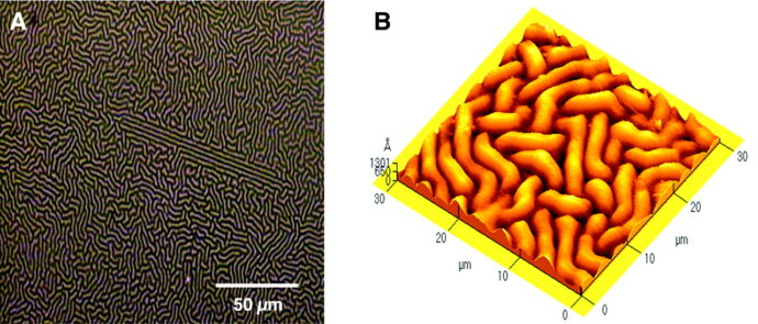
To assess CMP wafer quality, manufacturers utilize a range of testing and characterization methods. Surface profilometry is commonly used to measure surface roughness and planarity. Optical microscopy and scanning electron microscopy (SEM) are employed to inspect the wafer surface for defects, scratches, or contamination. Analytical techniques such as X-ray photoelectron spectroscopy (XPS) and secondary ion mass spectrometry (SIMS) are utilized to analyze the chemical composition and impurity levels on the wafer surface. These comprehensive evaluations ensure that these devices meet the required specifications and deliver consistent performance.
Emerging Trends and Future Outlook
The field of CMP wafers is constantly evolving, driven by emerging trends and ongoing research. These developments shape the future of these devices and their implications on device precision.
Current Trends Shaping the Field of CMP Wafers
One of the current trends in CMP wafer technology is the development of environmentally friendly slurries that reduce chemical waste and improve recyclability. The integration of advanced metrology techniques and real-time process monitoring is another emerging trend, enabling better control and optimization of all processes. Additionally, there is a growing demand for CMP wafers tailored for advanced packaging technologies and heterogeneous integration as the semiconductor industry embraces new device architectures.
Potential Future Developments and Their Implications on Device Precision

Looking ahead, the future of CMP wafers holds exciting possibilities. Continued advancements in polishing pad materials and slurries will enable even higher levels of precision and control over material removal. The integration of artificial intelligence (AI) and machine learning algorithms in these processes could optimize polishing parameters and improve efficiency. Furthermore, the development of CMP wafers with advanced functionality, such as self-healing surfaces or surface modification capabilities, could further enhance device performance and customization.
Conclusion
CMP wafers play a significant role in achieving precision and enhancing semiconductor device performance. Their contribution in achieving uniformity, minimizing defects, controlling surface topography, and customizing surface properties is paramount in the fabrication process. Ongoing advancements and research in CMP wafer technology are essential to meet the increasing demands of the semiconductor industry and continue pushing the boundaries of device precision. As the field evolves, the importance of CMP wafers in achieving precision and enhancing semiconductor device performance will remain a key focus, enabling the development of more advanced and powerful technologies in the future.


